Modeling of Die Surface Features on Integrated Circuits to Improve Device Reliability
by John SauberTable of Contents
- Abstract
- Introduction
- Statement of Problem
- Analysis Method
- Results
- Conclusions
- Summary
- Acknowlegements
- References
Abstract
When semiconductor devices are encapsulated in plastic, the glass-like dielectric
and passivation layers on the surface of the die are subjected to very high
stresses from the shrinkage of the molding compound. This paper reviews the
modeling approach used to simulate very small features (~0.1 mm) inside of a
relatively large (~28000 mm) package, with the goal of optimizing the design
to eliminate device failure caused by cracking of the dielectric and passivation
layers.
Introduction
A complex stress state exists inside of a semiconductor device caused by the
series of process steps which is used in its fabrication. A large single crystal
of silicon is sliced into wafers which are typically 6" to 8" in diameter,
but only 0.011" to 0.024" thick. Using vapor deposition and photo-imageable
masking technology, alternating layers of aluminum and glass-like PETEOS dielectric
(Plasma Enhanced TetraEthylOrthoSilicate, commonly called "oxide")
are applied to the surface of the wafer. Since these layers are deposited at
high temperatures (340°C to 390°C) and since the aluminum and the
oxide have very different thermal expansion coefficients (23 ppm/°C and
0.5 ppm/°C respectively) a great deal of intrinsic stress is generated
when the devices are cooled to room temperature.
After depositing a final "passivation layer" of silicon nitride (Si3N4, commonly called "nitride") to protect the circuits from moisture, the wafer is sawed apart to singulate the individual dies. The dies are tested electrically, and then installed into a package which is typically made of either ceramic (for high power/high cost devices) or plastic (for low power/low cost devices). For plastic packaging, the die is mounted on the "die pad" portion of a copper leadframe using an epoxy adhesive, and then connected electrically to the "bond fingers" in the leadframe using fine (0.001" diameter) gold bond wires as shown in Figure 1. The leadframe/die assembly is then encapsulated in a silica filled, Novolac epoxy molding compound using a transfer molding process.
Statement
of Problem
As previously mentioned, the die fabrication process creates high intrinsic
stresses in the dielectric layers, the aluminum lines and the passivation layer
on the surface of the die. When the die is encapsulated, additional stresses
are generated by the expansion differential between the die and molding compound
as the device cools to room temperature. To further complicate the issue, the
adhesive bond between the molding compound sometimes will fail (delaminate)
which can concentrate the forces and stresses on the various features on the
die's surface. If the stresses are high enough, it is possible for the passivation
layer and/or the dielectric layers to crack. Once this has occurred, moisture
can penetrate into the aluminum lines which can cause corrosion which can lead
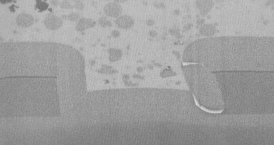
to failure. Focused Ion Beam (FIB) technology was used to expose the inside
of the die surface revealing the cracked dielectric and passivation layers shown
in Figure 2.
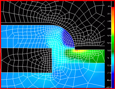
Analysis
Method--Models
The difficulty with modeling this structure is that the features which are of
interest are very small, requiring elements which are only ~0.1 mm on a side.
To put this in perspective, a human hair is typically about 75 mm in diameter.
The device itself is a relatively large 28,000 mm across, and since interactions
between the various components in the package have a direct effect on the stresses
on the die surface, the whole package must be modeled. While it is possible
to solve this problem using submodeling [1,2], the Mesh Paver (automatic
surface mesher) utility in MSC.Patran makes it fairly simple to model the
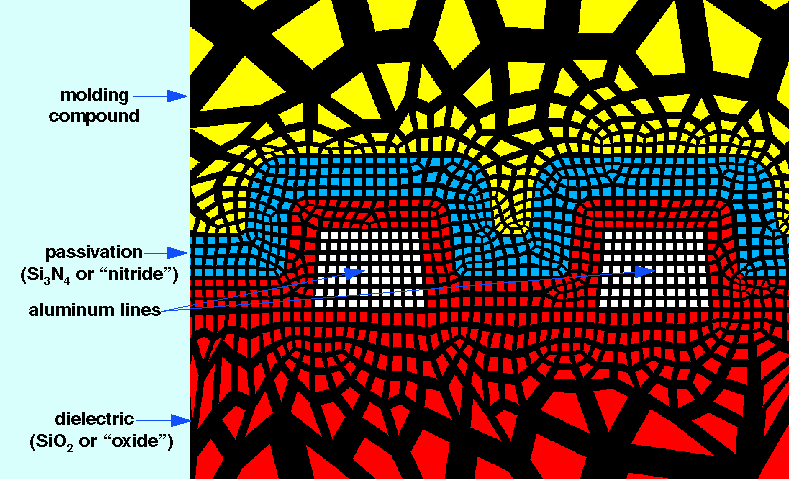
entire structure. Figures 3, 4,
and 5 show how the package is modeled.
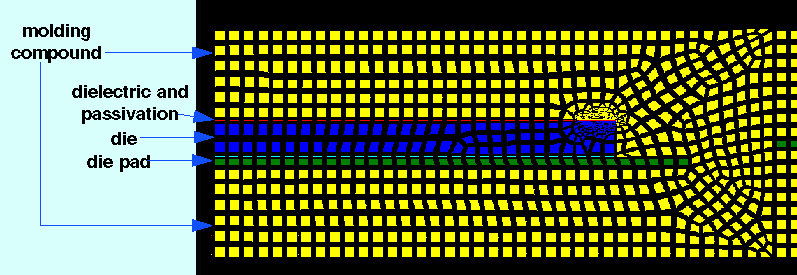
Figure 3 -- Model of a diagonal cross section of the package (12K)
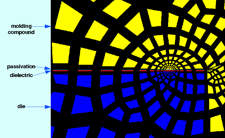
Figure 4 -- Close-up of corner of die (14K)
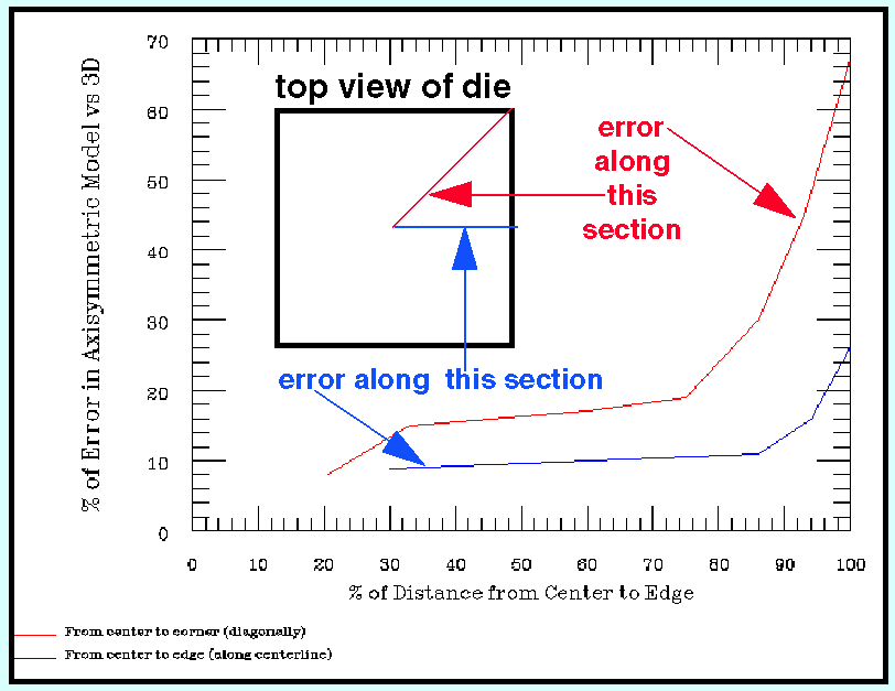
MSC/ABAQUS 4 node axisymmetric elements (CAX4) were used. It was necessary to use a 2-D approximation because any 3-D model fine enough to include the sub-micron features would have required such a large amount of solution time that our funding would have expired before any results were obtained. Since this is actually simulating a disk shaped die instead of a square die, a study was conducted to determine the amount of error caused by the approximation. A 3-D model of the device was built using elements which were .005" (127 mm) on a side. Two axisymmetric models were built of the same device, one simulating a section from the center to the edge of the package, the other simulating a section from the center to the corner of the package. The amount of error in the Von Mises stress in the passivation layer for the two axisymmetric models compared to the 3-D model is shown in Figure 6 (15K) as a function of location (normalized distance from the center of the die).
Not surprisingly, both of the axisymmetric models were fairly accurate near the center of the die. The center-to-edge model was accurate across most of the die surface, and was only off by 26% at the edge of the die. The center-to-corner model was off by considerably more, producing an error of 67% in the very corner of the die. Examining the source of the error showed that the center-to-corner model was not taking into account the "squeezing" effect that the molding compound exerts on the corner of the die. Fortunately, the goals of the project only required that we evaluate the relative merits of various design options. Since the features to be evaluated were all located on the same small section of the die surface, the results produced would be acceptable for comparing the relative impact of design changes to those features.
The use of the economical axisymmetric elements proved to be quite important. Even though typical models had anywhere from 6,000 and 11,000 elements, our Digital AlphaStation 600 5/266 workstation was able to solve them in only 1 or 2 minutes per iteration. However, the contact surfaces needed to simulate interfacial delamination required dozens of iterations per load case to converge, and many load cases were needed to quantify the effects of the many design variables, so hundreds of iterations had to be solved to complete the project. This would not have been possible if a 3-D modeling approach had been used.
Analysis Method--Material PropertiesThe SRC/CINDAS Microelectronics Packaging Materials Database [3] was used to find the properties of the various materials. The properties of the aluminum, dielectric and passivation were derived from testing of thin film materials which were deposited using processes that were identical to those used in actual production. This is an important detail since thin film properties are often quite different from bulk properties. Analysis Method--Accuracy
The ability of the model to accurately predict the stresses in the dielectric and passivation was verified by examining the stresses in areas of the die surface which do not contain any metal lines. The CINDAS database includes data on nitride or oxide film stress (F.S.) calculated from wafer curvature measurements by using the following equation:

Where E is the Young's modulus for the Si substrate, N is its poisson's ratio, D is the thickness of substrate, t is the film thickness, and R is the net radius of curvature. Digital also routinely conducts these tests as a method for process control, and obtains the same results that CINDAS does. Models built of an oxide-only or nitride-only film over silicon provide extremely good correlation with oxide stresses being within 1% and nitride stresses being within 10% of the published values. While this does not insure that every result for every metal line structure is correct, it does provide a good "sanity check" on the material properties and loading conditions.
Analysis Method--Modeling
Procedure
In order to simulate the assembly procedure, the analysis must be done in three
steps:
1. The entire finished assembly
is modeled, but the modulus of the molding compound is set to a very low number
so that it is essentially "invisible". This model is solved for cooling
from the dielectric / passivation deposition temperature (390°C) to the
molding temperature (150°C). The major principal stresses and deformed
shape for this step are shown in Figure 7:
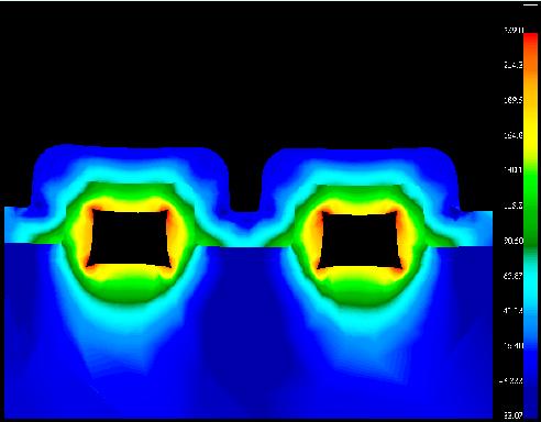
Figure 7 -- Cooling from 390C to 150C, no molding compound (21K)
2. The same model is solved for
cooling from the molding temperature (150°C) to room temperature, only
this time the actual molding compound properties are used as shown in Figure
8:
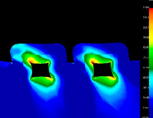
Figure 8 -- Cooling from 150C to 20C with molding compound (17K)
3. Since these are linear materials,
superposition can be used to combine the two load cases. Using the PATRAN post-processor,
the component stresses are combined and then the principal stresses are recalculated
as shown in Figure 9:
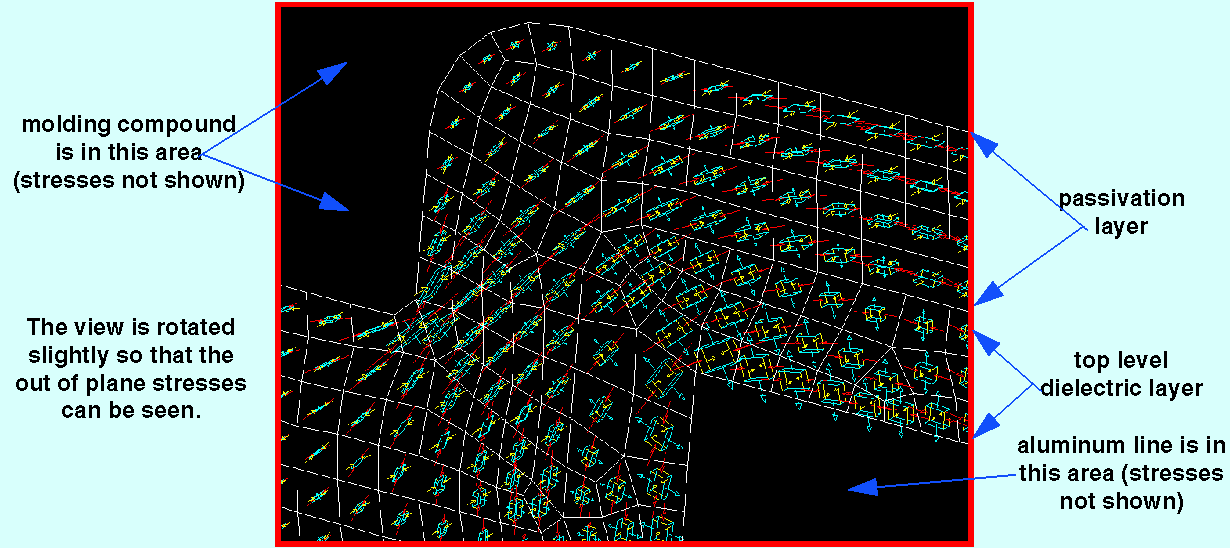
An examination of the principal stresses in the dielectric and passivation layer near the aluminum lines shows that the intermediate and minor principal stresses are mostly compressive, while the major principal stress is tensile. As is the case with many glass-like materials, the strength of the oxide and the nitride is much higher in compression than it is in tension, so, failure is most likely to be caused by the major principal stress. Figure 10 (40K) shows the directions of the principal stresses near the aluminum lines. The view is rotated slightly so that the out of plane stresses can be seen. The stresses in the line and the molding compound are not shown.
Results--Optimizing
Layer Thicknesses and Process Parameters
The analysis method was used to optimize the thicknesses and deposition temperatures
of the passivation and top dielectric layers, and to select the best material
choices for the molding compound. Response surface modeling using the RS1/Discover
software (trademark of Bolt, Beranek and Newman Inc.) was used to interpolate
between the variables. This approach minimizes the number of load cases which
must be solved to understand a problem which is affected by several variables.
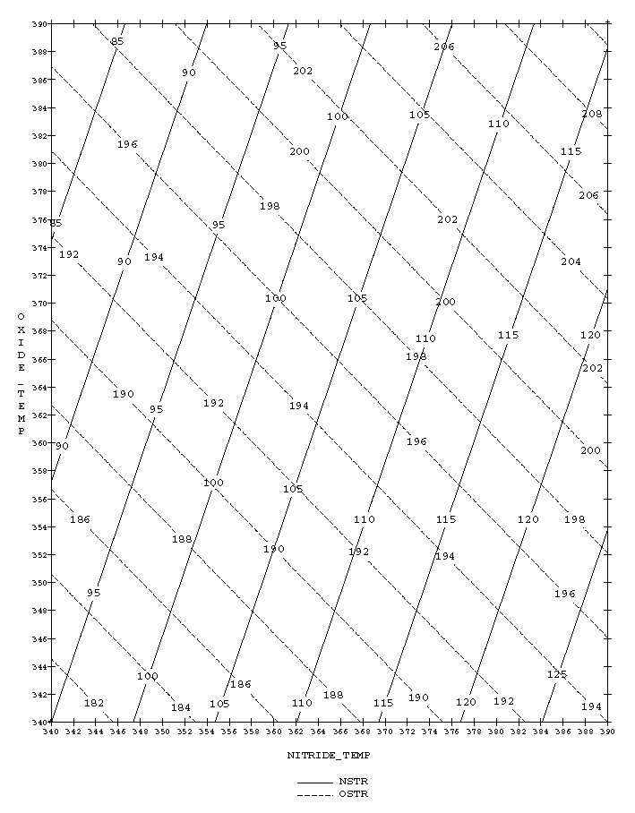
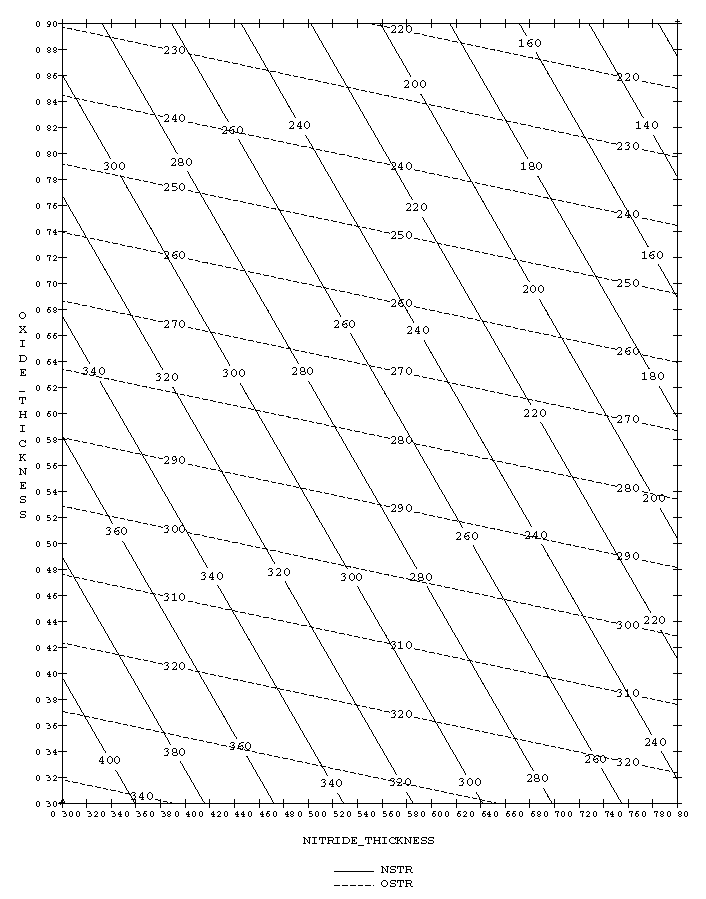
Figure 11 (18K) shows the impact of deposition
temperature on nitride and oxide stresses, while Figure
12 (18K) shows the effects of layer thickness.
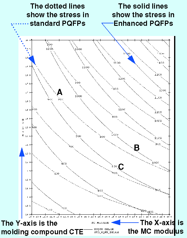
Results--The
Effects of Molding Compound Properties and Delamination
Scanning acoustic micrography (C-SCAN) results have shown that in some cases
a loss of adhesion (delamination) occurs between the molding compound and the
passivation layer. To simulate this condition, MSC.Abaqus contact surfaces were
used to allow sliding contact at the interface. Results were produced for both
the standard Plastic Quad Flat Pack (PQFP) and the thermally Enhanced PQFP which
contains a large copper heatspreader underneath the die pad. This study also
included an examination of the effects of molding compound CTE and modulus since
these are known to have an effect on the die surface stresses [2
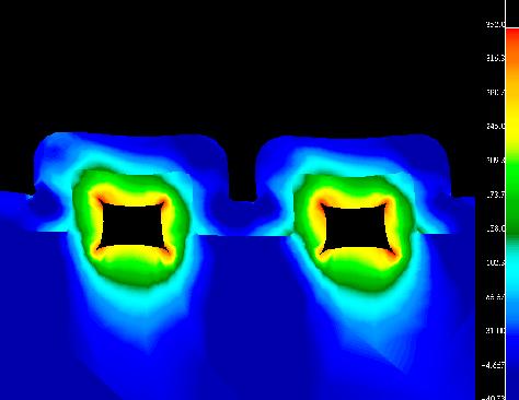
,6,7]. Figure
13 (28K) shows a typical deformed shape for the structure and the resulting
stress concentration in the passivation layer. The location of the peak tensile
stresses agrees with the failure mode observed by Lesk, et al [8]
in cases where molding compound / passivation delamination has occurred. Figure
14 (16K) shows a response surface graphs of the results. Points on the graph
show the various grades of molding compounds (i.e., "A", "B"
& "C") which are available.
Conclusions
Several conclusions can be drawn from these studies:
- Delamination has a huge effect resulting in a factor of 12 to 20 increase in passivation layer stresses. All other considerations are secondary compared to the need to eliminate or control the effects of delamination. Test results [9] have shown that delamination is one of the main causes of electrical failure. Delamination has also been shown to cause up to a 10 fold increase in the molding compound stress intensity factor which can result in cracking of the entire package [10].
- Reducing molding compound CTE from 20 to 10 ppm/°C reduces the nitride stress by anywhere from 32% to 56%
- Reducing molding compound modulus from 20 to 10 GPa reduces the nitride stress by anywhere from 22% to 40%
- The product of molding compound (CTE) x (modulus) is an effective indicator of the relative "goodness" of a molding compound. This relationship (which is sometimes referred to as the resin parameter) has been observed in test results from other researchers [11].
- Reducing die attach modulus
from 8 to 0.4 GPa reduces the nitride stress by:
- Anywhere from 8% to 11% for PQFPs
- Anywhere from 0% to 6% for EPQFPs
- Using a PQFP instead of an EPQFP reduces the nitride stress by anywhere from 6% to 28%
- Molding compound choices:
- Using molding compound C instead of A reduces the nitride stress by 7%
- Using molding compound A instead of B reduces the nitride stress by 5%
- Using molding compound C instead of B reduces the nitride stress by 12%
Several methods for controlling the effects of delamination have been modeled, built and tested, but since the patent process for these designs has not yet been completed they are considered proprietary and cannot be described in this paper.
Summary
An analysis method was developed for calculating the stresses which occur in
the top level dielectric and passivation layers on the surface of a semiconductor
die. The assembly process was simulated by solving load cases for the steps
before and after encapsulation, and then combining the results in the post-processor.
A series of models were solved to quantify the amount of error at various locations
on the die caused by using an axisymmetric approximation of the structure. The
method was used to identify the optimum layer thicknesses and deposition temperatures
for minimizing the dielectric and passivation layer stresses. Models were built
with sliding surfaces to simulate delamination of the molding compound / passivation
layer interface. The differences between standard PQFP devices and thermally
Enhanced PQFPs were evaluated. Finally, a series of models were solved to determine
the effects of molding compound and die attach adhesive material properties,
and to select the best commercially available materials.
Acknowledgments
This work would not have been possible without the hard work and support shown
by many individuals. In particular the author would like to acknowledge the
contributions of Antonio Berti, Ahsan Enver, Wendy Fowler, Jim Gardner, Terri
Giversen, Jaime Ide, Larisa Kisselgof, John Kowaleski, Lidia Lee, Jeff Maggard,
Tom McCoy, Wade McFaddin, Hon Nguyen and Brian Walker.
References
1. Michael, M.M., "Stress analysis for large die plastic
packages", Proc. of the National Electronic Packaging and Production Conf.,
NEPCON East, 1991 pp. 435-445.
2. Pendse, R., and Demmin, J., "Test structures and finite element models for chip stress and plastic package reliability", Proc. International Conf. on Microelectronic Test Structures", 1990, pp. 155-160.
3. Center for Information and Numerical Data Analysis and Synthesis (CINDAS), Microelectronics Packaging Materials Database, Purdue University, developed under the sponsorship of the Semiconductor Research Corporation (SRC), Update #14, Sept. 1995.
4. Kato, H., Sakai, H. and Sugawara, K., "Microdefects in oxide films deposited on featured surfaces of VLSI substrates by thermal CVD of TEOS and O2", J. of Electrochem. Soc., Vol. 141, No. 11, Nov. 1994, pp. 3154-3157.
5. Wu, T., and O'Brien, K., "Comparison of passivation films: the effect of thermal cycles and comparison of phosphorous doped oxide films", J. of Vacuum Science Technology, B 11(6), Nov./Dec. 1993, pp. 2090-2095.
6. Foehringer, R., Golwalkar, S., Eskildsen, S. and Altimari, S., "Thin film cracking in plastic packages - analysis, model and improvements", Proc. 41st Electronic Components and Technology Conf. , 1991, pp. 759-765.
7. Zelenka, R., "A reliability model for interlayer dielectric cracking during temperature cycling", 29th Annual Proc. Reliability Physics, 1991, pp. 30-34.
8. Lesk, I., Thomas, R., Hawkins, G., Remmel, T., and Rugg, J., "Progression of damage caused by temperature cycling on a large die in a molded plastic package", Proc. 40th Electronic Components and Technology Conf., 1990, pp. 807-812.
9. Doorselaer, K., and Zeeuw, K., "Relationship between delamination and temperature-cycling induced failures in plastic packaged devices", Proc. 40th Electronic Components and Technology Conf., 1990, pp. 813-817.
10. Sauber, J., Lee, L., Hsu, S., and Hongsmatip, T., "Fracture properties of molding compound materials for IC plastic packaging", IEEE Transactions on Components, Packaging and Manufacturing Technology, Vol 17, No. 4, Dec. 1994, pp. 533-541.
11. Miura, H., Nishimura, A. and Kawai, S., "Structural effect of IC plastic package on residual stress in silicon chips", Proc. 40th Electronic Components and Technology Conf., 1990, pp. 316-321.